A shortcut to the world of point-of-care diagnostics: Optimization for miniaturized foil-based microfluidic chips

A shortcut to the world of point-of-care diagnostics: Optimization for miniaturized foil-based microfluidic chips

Task

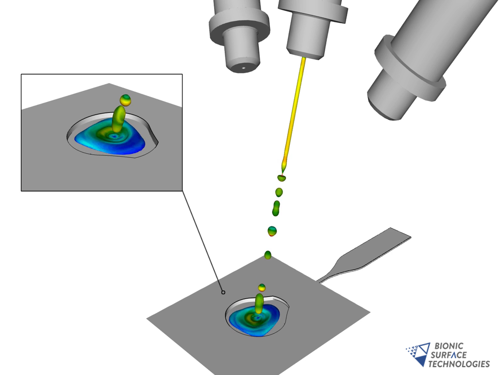
Improvement. The chip was designed to detect pathogens/anti-bodies in a point-of-care setting. The presence of air bubbles when filling the chip with a fluid was investigated.

Solution

Verification of several hypothesis what causes the air bubbles by means of numerical simulation. The theory that spots in the fluid channel resulted from sudden contact angle changes proved true.

Benefit

No need to run several expensive and time-consuming test series to find out the cause as the simulation yielded an unambiguous result.

Image
Project details
The project objective was to develop a microfluidic chip design for the detection of pathogens/anti-bodies for GENSPEED Biotech GmbH. GENSPEED is a biomedical company which produces and distributes in-vitro-diagnostic-certified rapid testing solutions offering easy and fast detection of pathogens or biomarkers at the point-of-care within minutes. A combination of microfluidics, miniaturized opto-electronics and automation builds the basis of a completely new, small, and simple test system.
Within the last few years, a tremendous technological advancement in the chip design took place giving way to a miniaturizing process. Miniaturization is a driving force for an innovation in diagnostics, which is called “lab-on-a-chip.” The use of micro- and nanotechnologies allows the development of fast, portable, and easy-to-use systems. The conventionally used commercial chips, produced by melt injection, became gradually replaced by fully foil-based-chips. The former chips had a thickness of 5mm while the new lab-on-foil-chips manage with less than 0,2mm! The special feature is the design of tiny microfluidic channels on thin and flexible foils The microfluidic channels are created by using nanoimprint lithography by means of a roll-to-roll process. That process prepared the ground for an unseen miniaturizing of test kits allowing mass production of such lab-on-chip systems. A development which combines many advantages: a cheap, fast and easy scalable production process which beats the formerly used commercial chips production by lengths. However, the miniaturizing process throwing up some unexpected challenges. One new challenge to address was the presence of air bubbles when filling the chip with a fluid. We had to find out why the air bubbles occurred and to propose a solution.

Cause studies can be carried out by testing theory by theory in-situ. The smarter and more cost-efficient way is to run individual simulations. Simulating has the huge advantage that you can verify different hypothesis without running any test at all. Thus, limiting the time and cost amount spent on testing capacities considerably. In the present case the microfluidic chip consisted of multi-layered foils. As the foils had either hydrophobic or hydrophilic characteristics small defects in the laminating layer in the manufacturing process produced irritations. The air bubbles therefore were a result of hydrophobicity as the microfluidic flow rose in the fluid channel with hydrophilic properties due to the capillary effect. Even small areas with surface defects in the laminate layer produced the well-known lotus effect. The fluid flowed faster sideways on the hydrophilic solid surface whereas it flushed around the air bubbles, as the illustration below clearly shows. By means of simulation we proved true that changes in the contact angle of the surface were responsible for the air entrapment – the bubbles.

Outcome
We found the reason for the presence of air bubbles by means of numerical simulations. Furthermore, based on a sensitivity analysis we were able to show which surface parameters had an influence on the results. Numerical simulations allowed us to come across two unexpected results: The fact that even small contact angel changes resulted in the presence of air bubbles. And, even more surprisingly, that the defective areas did not necessarily have hydrophobic properties. The collected data regarding the flow pattern and the sudden changes in the contact angle serve as a basis for optimizing the manufacturing process to avoid result relevant errors in the future. The benefits for GENSPEED are obvious: A viable solution while at the same time minimizing time and cost expenditures.
Image